
How SoC FPAA Technology is Bringing Analog Computing to the Frontlines of Defense Systems
In an increasingly digital world, the whisper of analog computation might seem like a relic of a bygone era. Yet, beneath the sleek facades of our smartphones, satellites and autonomous vehicles lies a quietly powerful movement: fieldprogrammable analog arrays (FPAAs). Today, with the recent acquisition of Anadign by OKIKA Semiconductor, we stand at the threshold of a new age in mixedsignal, systemonchip (SoC) design—one where analog circuits are as reconfigurable as their digital cousins, and the line between physics and code blurs in service of ultraefficient, realworld needs.
From Silicon Labs to the Physics Lab Bench
Professor Jennifer Hasler, a pioneer in “physical computing,” recounts the moment she realized the potential of largescale analog reconfiguration. While exploring neuromorphic architectures in the early 2010s, she and her students discovered that analog circuits—long dismissed as unforgiving and inflexible—could be tamed with modern calibration, compact standardcell libraries and floatinggate memory elements. By 2016, her team had demonstrated a 1,000× reduction in energy per operation compared to digital equivalents—a landmark achievement that would set the stage for today’s SoC FPAA renaissance.
Yet, until recently, designers faced a dizzying toolchain: custom layout, painstaking tuning, and a lack of systemlevel support kept analog squarely in the realm of specialists. That is, until OKIKA’s engineers and Anadign’s analog designers joined forces.
OKIKA + Anadign: Forging the Future of MixedSignal SoCs
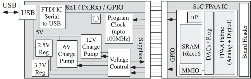
When OKIKA Semiconductor announced its acquisition of Anadign last year, the industry took notice. Anadign’s configurable analog blocks (CABS) and highdensity floatinggate SRAM IP—once available only to bleedingedge—became part of OKIKA’s venerable SoC portfolio. The result: a family of SoC FPAAs that pair digital processing cores, power management and RF front ends with reprogrammable analog cells, all under a unified toolchain.
At the heart of the new OKIKA SoC FPAA lies a grid of precisiontunable conductors and capacitors, arranged in a compact fabric that fits within a 20 nm process node. Each analog “tile” supports continuoustime filters, oscillators and nonlinear functions, while reconfigurable interconnect ensures seamless routing between analog, digital and RF domains. Beneath the surface, a lightweight SRAM bank stores both analog configuration words and code, allowing dynamic reprogramming in the field.
OKIKA’s vision is clear: deliver an “analog GPU” on a single chip—capable of performing tens of teraMACs per second in RF signal processing or sensor fusion, with power envelopes measured in milliwatts.
Why Choose an SoC FPAA? Beyond the FPGA vs. GPU Debate
For decades, system designers have relied on fieldprogrammable gate arrays (FPGAs) and GPUs to accelerate computeintensive tasks. Yet both architectures share a digital lineage that carries intrinsic inefficiencies when interfacing with the analog world. Converting realworld signals to bits, processing them, then converting back consumes precious power and adds latency.
Enter the SoC FPAA: by computing directly on voltage and current, these devices circumvent the power-hungry analogtodigital converters and digital signal processors. In OKIKA’s latest devices, a programmed filter or classifier runs at 1,000× energy efficiency compared to a comparable digital design, and occupies just oneeighth the die area of a GPU or FPGA implementation at 20 nm. With up to 10–100 million analog “gates” available, designers can map entire sensor-processing pipelines—feature extraction, classification and control loops—entirely in the analog domain.
Take, for example, an auditory classifier embedded in a wireless sensor node. Traditional DSP approaches require digitizing audio, running computeheavy spectral transforms on a microcontroller or GPU, then classifying the result. OKIKA’s SoC FPAA, by contrast, tunes a bank of analog filters and threshold detectors to extract pitch, loudness and temporal features—all in real time, at a handful of microwatts. The result: a batterypowered node that can monitor environmental noise for weeks on a coincell battery.
Building Real Systems: Tools, Workflows and Ecosystems
A common refrain among analog skeptics: “Sure, it works on a lab bench, but can I actually build a product?” OKIKA’s answer is a resounding “yes.” Alongside the SoC FPAA, the company provides a comprehensive tool suite—OKIAnalog Studio—that offers schematic capture, corneraware simulation, and auto-generated calibration routines for process, voltage and temperature variations.
Under the hood, the toolchain leverages a mixedmode simulator codeveloped with Professor Hasler’s group, integrating analog behavioral models with registertransfer level (RTL) descriptions of onchip digital accelerators. Once a design is verified, the same environment deploys configuration bitstreams to hardware via JTAG or even overtheair firmware updates.
OKIAnalog Studio’s draganddrop blocks include auditory front ends, matched filters, finitestate machines, floatinggate neural cells and powermanagement controllers—each parameterized for area, speed and power. For rapid prototyping, designers can spin up evaluation boards featuring the SoC FPAA, an FPGA for glue logic and a microcontroller for highlevel orchestration. The result is a real system in days, not months.
Field Programmable Analog Arrays (FPAAs) are enabling new levels of adaptability in harsh signal environments, particularly underwater imaging. In these systems—used in everything from fish finders to advanced naval sonar—conditions such as temperature gradients and suspended sediments make clear imaging a challenge. Anadigm FPAAs allow real-time, dynamic reconfiguration of sonar filters, enabling the system to adjust to changing acoustic conditions without hardware modifications. This flexibility continues to represent the cutting edge in reconfigurable analog signal processing.
Spotlight on Capabilities: From State Machines to Analog GPUs
The versatility of the SoC FPAA shines through in its range of “IPMAC” capabilities (analog multiplyaccumulate per second). OKIKA’s flagship device boasts 10 TMAC/s in a singlechip module—an analog GPU designed for RF signal chain tasks such as beamforming, chirp detection and spectral scanning. Paired with onchip ADCs and DACs, the FPAA can perform realtime modulationdomain filtering, adaptive equalization and even dynamic poweramplifier linearization without offchip support.
On the simpler end of the spectrum, designers can implement robust finitestate machines entirely in analog blocks. Imagine an ultralowpower sensor that wakes only when a sequence of temperature and vibration thresholds fire in a particular order—no microcontroller needed. The analog FG (floatinggate) programming technology, pioneered by Hasler’s team, ensures nonvolatile state retention across power cycles, with energy costs measured in nanojoules per write.
The Road Ahead: Scaling to Millions of Gates
As with any semiconductor technology, scaling is key. OKIKA and Anadign’s combined IP roadmap targets 7 nm and below, with projections of 100 million analog gates on demand by 2026—an order of magnitude increase over today’s offerings. At those densities, entire neural network accelerators and adaptive control systems will fit alongside digital cores on the same die, pushing analog computing into the mainstream of edgeAI and 5G/6G RF domains.
Looking further out, there’s talk of cryogenic FPAA fabrics for quantum-control electronics—leveraging the ultralowtemperature performance of floatinggate CMOS circuits to orchestrate qubit arrays. If realized, such devices could dissolve the hardware barrier to practical quantum computers, embedding control loops directly at millikelvin temperatures.
When You Grow Up: The AnalogDigital Convergence
Ask any SoC architect where the next wave of innovation will come from, and the consensus is clear: convergence. The dichotomy between analog and digital is giving way to a continuum of computation across the electrical spectrum. OKIKA’s SoC FPAA, born of a union with Anadign and guided by the vision of Jennifer Hasler, embodies that convergence—offering system designers the best of both worlds: the precision and reconfigurability of digital logic, married to the power efficiency and realworld intimacy of analog.
In the coming years, expect to see FPAApowered sensor nodes that last for decades on energy harvesting, RF frontends that adapt in real time to spectrum conditions, and autonomous robots whose senseandrespond loops operate entirely in the analog domain. The analog revolution that Professor Hasler foresaw is now at our doorstep—and with FPAASoCs from OKIKA, we have the tools to step boldly into that future.