

In military and aerospace systems, thin-film patterned substrates are often the foundation for the most critical electronic assemblies.
In military and aerospace systems, thin-film patterned substrates serve as the foundation for some of the most critical electronic assemblies, including RF, microwave, millimeter-wave, and high-speed digital circuits.
These substrates are typically made by depositing extremely thin layers of conductive and dielectric materials on bases made from materials such as alumina, aluminum nitride, quartz, or certain high-performance titanates with dielectric constants up to 4000.
The goal: to create precise, stable electrical pathways that improve electrical performance and increase reliability even under extreme conditions such as rapid temperature fluctuations, high vibration, exposure to radiation, and long mission lifetimes where maintenance is impossible. An additional benefit is that thin-film circuits are often smaller and lighter than those of other technologies, which can be important for airborne and spaceborne systems.
This level of precision is essential for electronics embedded in low-earth orbit (LEO) satellites, drones, spaceborne communications, radar payloads, navigation systems, and signal-processing electronics, where even slight impedance or phase shifts can degrade link quality, reduce antenna beam accuracy, or impair payload measurements.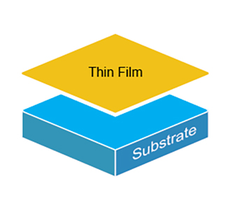
Thin Film Substrates
Compared to thick-film or regular printed circuit boards, thin-film technology allows for extremely fine detail, often with lines and spaces just a few microns wide, helping ensure electrical performance is consistent from one part to the next.
With accurate conductor line widths and spacing, designers can control the characteristic impedance of transmission lines, RF trace coupling, and even thermal loads within RF circuits.
At high frequencies, even a small change in the width of a circuit trace can affect impedance or detune a filter, so this level of control is critical. It also allows more circuitry to fit into a smaller space while keeping unwanted electrical effects to a minimum.
“Functionally, thin film substrates provide the stable, high-precision electrical platform on which critical aerospace and military electronics are built. They allow complex circuits to be integrated in ways that minimize signal loss, maintain phase coherence, and reduce noise—attributes that directly impact range, clarity, and security of communications, as well as the resolution and accuracy of sensing systems,” says Scott Horton of Johanson Technology. For more than 60 Years, Johanson Technology of Camarillo, Calif., has designed and manufactured passive components and substrates, including thin-film circuits, multi-layer ceramic capacitors, EMI filters, and other critical components for high-reliability applications.
Military and Aerospace-Grade Versions
Compared to commercial RF substrates, those for military and aerospace are manufactured to tighter dimensional tolerances and undergo more extensive screening. This includes controlling the dielectric constant, measuring conductor thickness with micron precision, and stress testing for vibration, shock, and thermal cycling.
High-purity gold, platinum, or other noble metals are often used for conductors to ensure low resistive loss, corrosion resistance, and consistent performance over decades. The dielectric layers are also applied with precise thickness control to achieve exact impedance targets and reduce parasitics, which is critical for multi-gigahertz wireless operation.
Space-qualified thin-film substrates are manufactured to far tighter tolerances and undergo extensive screening/testing before integration. This includes thermal cycling, random vibration, and shock testing to ensure performance.
Across all these military and aerospace applications, thin-film patterned substrates are designed. They can be screened to the highest-level reliability standards, such as MIL-PRF-38534 for hybrid microcircuits and MIL-STD-883 for environmental and mechanical stress testing.
“This combination of precision, thermal performance, and rugged construction makes them one of the few substrate technologies capable of meeting the performance and reliability expectations of modern defense and space electronics,” says Horton.
Substrate Selection
Horton adds that selecting the correct substrate is key because it influences the mechanical and electrical functions of a design.
Johanson Technology offers several dielectric k values and different metallization schemes to meet customer needs. The substrates can be metalized or nonmetallized. Metalized substrates can be patterned to customer specifications by chemical etching, abrasive etching, and patterned plating.
Single- or double-sided metallization is available, and each side can have unique design requirements and metallization for specific uses.
Adhesion layers such as titanium-tungsten or chromium help the metal adhere firmly to the ceramic, while gold, copper, or nickel provide good conductivity, solderability, and compatibility with wire bonding. The thickness of the gold layer is controlled to ensure wire bonds remain strong over time.
Attention should also be given to the coefficient of thermal expansion (CTE) and thermal conductivity parameters of the circuits involved. Spaceborne applications can experience large temperature swings from external sources (e.g., solar radiation), while higher-power systems can reach higher operating temperatures. These higher temperatures must be mitigated during the design process.
Aluminum nitride, specifically, conducts heat extremely well, spreading it away from hot components and helping them last longer, while alumina offers strong mechanical stability and high-voltage tolerance. Special “filled vias” inside the substrate reduce thermal resistance and electrical inductance, helping with heat transfer and maintaining clean signal paths.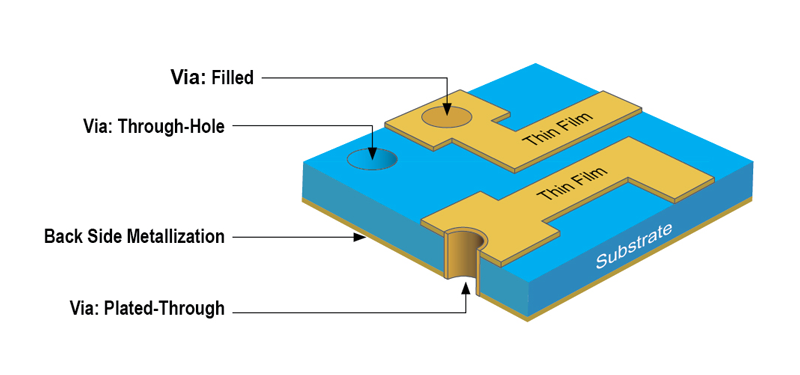
“In applications where heat conduction is critical, such as in the vacuum of space, designers must consider thermal conductivity of available substrates or use filled-vias as an alternative thermal path within a design,” says Horton.
Johanson Technology also has advanced experience in incorporating vias into substrate designs with demanding requirements. Vias can be offered as either filled, through-hole, or plated-through. The process involves drilling a hole through the substrate from the top to the bottom layer, then sputtering or plating over the substrate through the opening. Both options are effective for routing electrical signals from one side to the other.
“Plated-through vias are often recommended for low-power applications, while filled vias are ideal for high-power applications because they help transfer heat away from the substrate. Filled-vias also offer the lowest RF inductance,” says Horton.
Military and Aerospace Applications
Across the defense and aerospace sectors, numerous applications stand to benefit from the exceptional reliability offered by thin-film substrate technologies.
In LEO satellites, thin-film substrates often form the foundation for transceiver modules, frequency converters, phased-array control circuits, and sensor readout electronics.
In LEO, substrates undergo repeated thermal cycling every 90 minutes as the spacecraft moves in and out of sunlight, experiences exposure to vacuum, and is bombarded by radiation. These factors can cause dimensional changes, shifts in dielectric properties, or microcracking in poorly matched materials.
Reliability is therefore critical because satellites cannot be repaired once in orbit, and any electrical drift can have serious consequences.
For drones, the ability to integrate precision RF and high-speed digital components in a small footprint directly translates into more capable payloads without increasing size or mass, an essential factor in maximizing endurance and maneuverability.
In surveillance drones, thin-film substrates are used in microwave circuits for synthetic aperture radar or high-resolution imaging payloads. In strike drones, they might be part of encrypted communication modules or electronic countermeasure systems. Even in smaller tactical drones, they may be embedded in compact GPS receivers or advanced telemetry systems to ensure reliable navigation and data links.
Thin Film Substrates in Radar Systems: Military ground-based radar, shipborne radar, and airborne radar all rely on consistent RF performance, since small electrical variations can cause significant degradation in system performance.
In phased-array radar (T/R) modules, thin-film substrates enable long-range detection, high resolution, and resistance to jamming.
In active electronically scanned arrays (AESA), each transmit/receive module must handle high-frequency RF signals with precise phase and amplitude control. The fine-line tolerances of thin-film patterned substrates ensure that microstrip or coplanar lines have predictable impedance and minimal loss, so beam steering and radar resolution remain consistent across hundreds or thousands of modules.
In satellite and space communications payloads, thin-film patterned substrates are critical because they combine high-frequency capability with survivability in vacuum and radiation environments.
Aluminum nitride-based thin-film boards, for example, can efficiently dissipate heat from high-power amplifiers while maintaining structural stability through the extreme thermal cycles of orbit, ranging from −150 °C in shadow to +150 °C in sunlight.
Space-qualified versions of these substrates must comply with NASA’s EEE-INST-002 or the European ECSS-Q-ST-60 guidelines, which cover material selection, metallization thickness, adhesion strength, and environmental testing.
Avionics and flight control electronics also make heavy use of thin-film patterned substrates. Precision navigation systems, sensor processing units, and communications modules often operate in environments with constant vibration, rapid altitude changes, and wide temperature swings. The controlled thermal expansion of ceramics such as alumina and aluminum nitride reduces mechanical stress on the circuitry, helping prevent cracking or delamination over time. This is especially important for components mounted near engines or in other high-heat zones.
The compact, high-frequency RF circuits used in radar seekers, infrared seekers, or GPS receivers benefit from the low loss and tight impedance control of thin-film technology, which ensures targeting accuracy even after prolonged storage and during the extreme acceleration of launch.
Thin film substrates also play a critical role in electronic warfare (EW) and jamming systems. A substrate that shifts in impedance or resonant frequency due to thermal expansion, mechanical stress, or moisture ingress could instantly reduce jamming effectiveness or allow an enemy radar to regain a track.
By minimizing loss, preserving phase and amplitude accuracy, and resisting environmental drift, they ensure that a jammer can place energy exactly where it’s needed in the spectrum while keeping friendly systems free from self-interference. This combination of precision and durability is what enables EW platforms to operate effectively in the crowded, contested electromagnetic battlespace.
Functionally, thin-film substrates in radios and SATCOM systems enable compact, lightweight, and precisely tuned RF modules that maintain link quality, frequency stability, and filtering performance even under extreme environmental conditions.
By minimizing insertion loss, preserving phase accuracy, and allowing for complex multi-function integration in a small footprint, they ensure that communication links—whether between aircraft, ground forces, ships, or satellites—remain clear, secure, and reliable in mission-critical operations.
Because they support extremely fine conductor geometries with tight tolerances, thin-film substrates enable the high levels of miniaturization required for antenna feed networks, RF amplifiers, radar front ends, GPS modules, high-frequency filters, and phased-array control electronics.
In LEO satellites, drones, radar systems, and advanced communications equipment, these substrates provide the precision and long-term stability essential for RF, microwave, and high-speed digital circuits to perform reliably throughout the entire mission life.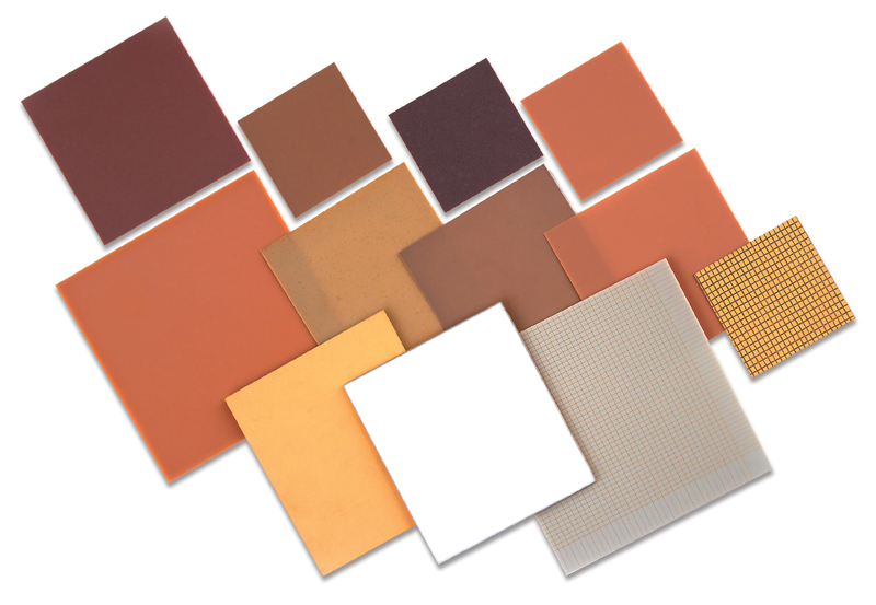
For more information, contact Johanson Technology at (805) 389-1166, visit the website at https://www.johansontechnology.com/ppr/military-aerospace/, or e-mail kvilla@johansontechnology.com. The company is located at 4001 Calle Tecate, Camarillo, CA 93012.