Contactless touch – a safer method for interaction
The ubiquitous smartphone is driving the demand and acceptance for touch as a method of interaction with electronic devices. Touch controls are now present in all parts of our daily lives. At home, we use touch to interact with our phones and home appliances; at work, whether in an office, retail store, hospital, or heavy industry plant, we are likely to use touchscreens or touchpads. Touch interaction is also finding its way into public areas such as elevator buttons, vending machines, information boards, and ordering screens in fast food restaurants.
However, there are instances where we hesitate to touch the interaction surface. We may want to avoid soiling it with greasy, dirty fingers or avoid the risk of being contaminated by anything residing on the surface. Making the interaction area hover over the screen/surface enables the familiarity of touch interaction without actually being in contact with the screen.
Introduction
Over the years, there have been recurring media reports about sanitary problems with frequently used public surfaces [1-3]. A study performed at three hospitals in Toronto, Canada, revealed that significantly more bacteria existed on elevator buttons than on surfaces in the hospital bathrooms [4]. The authors suggest replacing the elevator buttons with touchless proximity sensors to mitigate the risk of pathogen transmission.
Another report revealed that fecal bacteria were found on the touchscreens of ordering machines in a fast food restaurant chain [5]. There are other instances when contactless interaction would be beneficial, ranging from clinical environments where the user’s fingers may be contaminated by blood, viruses, or bacteria to industrial locations where the user’s fingers are covered with oily or greasy substances that would leave opaque residues on the screen making the screen information unreadable after using it for just a short period of time.
Available technologies
As suggested above, proximity sensors could work well for simple interaction surfaces such as elevator buttons, but would not work for touchscreens that require a continuous interaction area in mid-air.
Time of flight
An alternative solution would be to use a time-of-flight technology to identify mid-air interactions above a touchscreen. Time-of-flight is a ranging technique that resolves the distance between the sensor and an object by measuring the time it takes for light to travel to an object and back to the sensor. The accuracy lies in the order of 1 cm, which makes it unsuitable for touch interaction purposes. It is possible to improve the accuracy, but that will generally be at the expense of the frame rate. Furthermore, this kind of sensor requires calibration and is sensitive to changes in temperature.
Traditional touch technologies
- Resistive touch technology is not an option as it requires physical contact between the user and the device.
- Projected capacitive touch technology could be tweaked to operate at a distance above the screen. It will however put restrictions as to what kind of objects could be used for touch operation and the accuracy and response behavior will differ between different objects.
- Traditional infrared touch requires a frame surrounding the screens with emitters on two adjacent sides and receivers on the opposing sides. The touch interactive area is raised from the screen by simply raising the frame around the screen. The resulting rim around the screen will not only be difficult to incorporate aesthetically in a device, it will also make the screen difficult to clean, thereby defeating one of the purposes for its introduction.
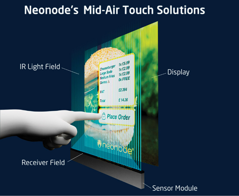
Infrared touch based on reflective technology
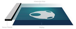
By using reflective technology, infrared touch can be implemented by mounting a sensor along one edge of a display. The interaction area consists of a sheet of light which is projected out of the sensor and positioned a desired distance above the surface of the display, see Figure 1.
Sensor geometry
The infrared touch sensor consists of an array of alternating emitters and receivers. Laser emitters are preferred over LEDs as they are easier to collimate and they generate less internal stray light within the sensor module. Any internal stray light needs to be kept to a minimum so that it does not interfere with the signal-generating light reflected from an object outside the detector. Vertical cavity surface emitting lasers (VCSELs) operating at 945 nm are used as emitters and silicon photodiodes are used as receivers.
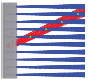
Molded polycarbonate lenses are used to collimate the light from the emitters and narrow the field of view of the receivers. By using shared optics for both the emitters and the receivers we force the receiver’s field of view to make an angle toward the direction of the emitted light, as shown in. This angle typically varies between 17 and 26 degrees depending on the aspect ratio of the sensor’s detection area.
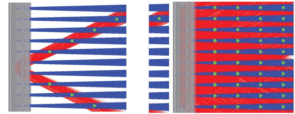
When adding multiple emitters, we can see the benefit of this geometry. Each receiver looks across several emitters and for each emitter there exists an area where the emitted light and the receiver’s field of view overlap, as shown in Error! Reference source not found.. It is only in this area that a detector can receive a signal from an object illuminated by the specific emitter. Outside this region, the detector won’t receive any signal at all.
Since each receiver is positioned between two emitters, the receiver will also detect light coming in through the optics shared with its other neighboring emitter, as shown in Figure 4 on next page. This enables us to generate a 2D-grid of regions of overlap.
Operational principles
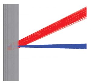
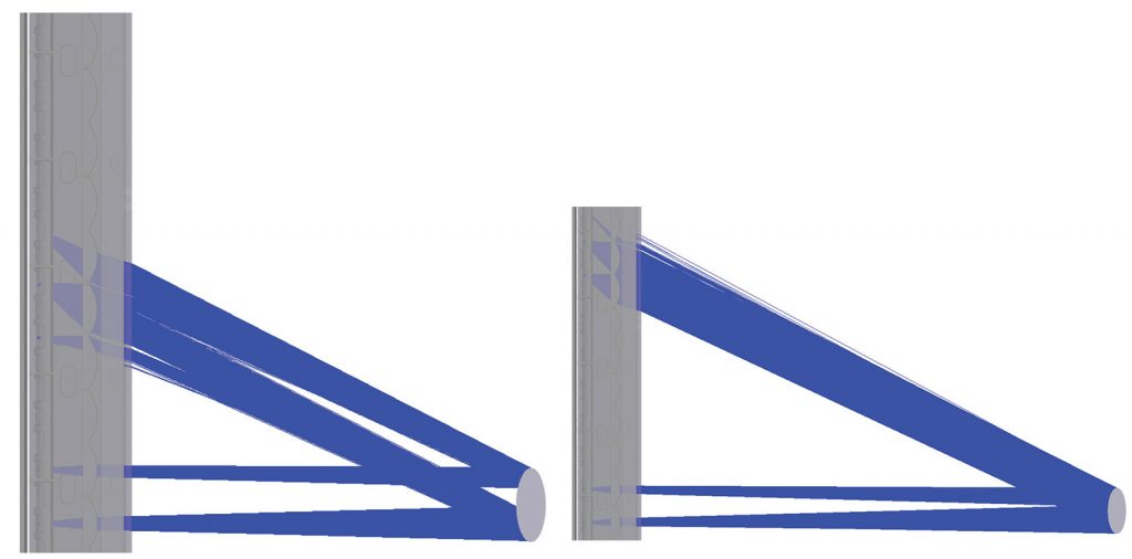
During a scan each emitter is scanned consecutively, while multiple receiver signals are recorded simultaneously. In contrast to infrared proximity detectors, which rely on signal strength for object positioning, the geometry of the sensor has turned object positioning into a geometrical question. An object’s position is determined based on which emitter-receiver combinations generate a signal during a scan. Figure 5 shows detection of an object close to the sensor along with detection of an object positioned further away from the sensor. Each detection is based on signals from two emitters and three receivers. The emitters are the same, but the receivers are different, which makes it possible to distinguish between the two object locations.
The accuracy of the sensor is somewhat dependent on the center to center distance between the regions of overlap for the emitted light and receiver field of view. However, the accuracy is improved by comparing the different signals. For any giving signal combination, the ratio between the signals from different emitters can be used to improve the lateral accuracy and the ratio between different receiver signals from the same emitter can be used to improve the distance accuracy.
Physical dimensions and electrical integration
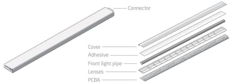
In order to accommodate for different display sizes, the sensor is available in different lengths ranging from 115 to 346mm. All sensors share a common width (14.5 mm) and thickness (3.46 mm). Figure 6 shows a detailed view of the sensor and its internal components. Electrical integration is performed via the connector at the edge of the PCBA. There are 8 contact pads and the PCB outline matches that of a standard 0.3-0.33 mm thick FFC/FPC with 1 mm pitch and top mounted connectors. This connection enables the sensor to communicate with a host system through a standard USB or I2C interface.
Conclusion
There are several occasions when it would be desirable to interact with a display or surface without actually touching it. Such contactless touch interaction can be provided with a sensor based on reflective infrared technology. The sensor projects a sheet of light that is responsive to touch. This sheet of light can then be raised above the display by controlling the spacing between the sensor and the display, resulting in a touch interaction area hovering above the display. This makes the display responsive to touch without any physical contact between the user and the display.
References
- Hospital elevator buttons show more germs than toilet stall surfaces, CBC News, July 8, 2014, Amina Zafar.
- The most germ-infested places you encounter every day — and how to avoid getting sick, Washington Post, December 14, 2017, Elisabeth Leamy.
- Investigation of Bacterial Pathogens on 70 Frequently Used Environmental Surfaces in a Large Urban U.S. University, Journal of Environmental Health Vol. 71, No. 6 (January/February 2009), pp. 17-22, Joanna S. Brooke, John W. Annand, Angela Hammer, Karen Dembkowski, Stanford T. Shulman.
- Elevator buttons as unrecognized sources of bacterial colonization in hospitals, Open Med. 2014; 8(3): e81–e86. Published online 2014 Jul 8. Christopher E. Kandel, Andrew E. Simor, Donald A. Redelmeier.
- Poo found on every McDonald’s touchscreen tested, Metro.co.uk, Nov 28, 2018, Adam Smith.
About the Author
Richard Berglind is a Senior Optical Engineer at Neonode and has more than 20 years of experience in various fields of optics. He holds a Master’s Degree in Engineering Physics from the Royal Institute of Technology, Stockholm, Sweden.