Phoenix Demonstrates Neutron Radiography Techniques for Product Inspection
For many electronics systems, especially in the aerospace, defense, and energy sectors, a critical feature is a certain degree of resistance to high-radiation environments. High-energy electromagnetic radiation such as gamma rays or energetic particles such as neutrons can wreak havoc on electronic infrastructure. As one might expect, neutron generators produce neutron radiation capable of causing damage to electronics, and so developing resilient, radiation-hardened electronics capable of having longer functional lifespans is critical for designing high-output systems. Phoenix, LLC, a nuclear technology company that builds compact, accelerator based high flux neutron generators, found itself in dire need of radiation survivability testing capabilities to further development of its systems. Since there are few facilities in which electronics can be subjected to intense levels of neutron radiation and monitored, Phoenix had to cultivate its own rad-hard and radiation effects testing capabilities in its neutron imaging facility in Fitchburg, Wisconsin to test and develop the electronics suitable for use in its most powerful systems.
How Radiation Damages Electronics
Ionizing radiation in particular, which is a type of radiation capable of stripping electrons away from atoms it comes in contact with, is particularly destructive to electronics. Alpha and beta particles are forms of directly ionizing radiation that possess their own electric charges (positive and negative, respectively) and thus interact strongly with matter and can ionize atoms simply by coming in contact with them. Gamma rays and neutrons, on the other hand, are forms of indirectly ionizing radiation that carry no charge of their own and interact much more weakly with matter, and cause atoms to become ionized either through phenomena such as the photoelectric effect and the Compton effect or by otherwise producing charged particles which themselves cause ionization.
These forms of radiation are profoundly damaging to the semiconductors you will find in any electronic system. When ionizing radiation strikes a semiconductor, it can remove some electrons in a process known as electron-hole pair generation. While this process is one of the fundamental phenomena behind the functioning of semiconductors in transistors, integrated circuits, and so on, when it happens as a result of exposure to ionizing radiation, it can lead to undesirable effects and eventually irrevocable damage.
A single charged particle knocking loose thousands of electrons can cause electronic noise or signal spikes that cause digital circuits to produce inaccurate or unintelligible results. Ionizing radiation can also cause lattice displacement that actually fundamentally changes the crystalline structure of the semiconductor and causes permanent physical damage.
High radiation levels, either in the form of powerful short-term pulses or long-term exposures, can cause random bit flips, change the logical states of memory cells, or cause electrostatic discharges. As a result, normal electronics will have severely shortened operational lifespans within high-radiation environments, resulting in equipment failing much sooner inside these environments compared to outside them.
Radiation Hardening of Electronics
Electronics used in spacecraft and satellites, defense systems, military aircraft, nuclear power stations, and other areas where exposure to high levels of ionizing radiation are likely must be designed to be sufficiently resilient to the effects of radiation so as to ensure that they will be able to function properly for a similar span of time as they would normally without the effects of radiation exposure. All electronics will begin behaving erratically and break down eventually as usage and entropy wear them down, but the damage caused specifically by radiation exposure will significantly hasten their demise. This can be mitigated through various means to ensure that electronics can remain healthy and functional with acceptable operational lifetimes.
One set of methods for rad-hardening electronics is to build them out of radiation-resistant materials. Certain materials can endure radiation exposure more effectively than the materials used in commercial-grade electronics. For example, rad-hardened chips can be manufactured on layers of insulating substrate instead of semiconductor wafers and thus can withstand orders of magnitude more radiation exposure. Bipolar integrated circuits can be used in favor of CMOS circuits, as the former have higher radiation tolerance than the latter in certain circumstances such as within amplifier circuits. Magnetoresistive random access memory can be employed, or capacitator based dynamic random access memory can be replaced with static RAM. The chips can be built on a substrate with higher tolerance to deep-level defects such as silicon carbide or shielded by radiation resistant materials. The boron-rich borophosphosilicate glass passivation layer protecting the chips can be manufactured using depleted boron to reduce the risk of neutron activation causing damage to the chips.
Another set of methods for rad-hardening electronics is less on the physical side and more on the logical side. Electronic systems can be designed with error-correcting code memory to check for and correct corrupt data, and can be built with multiple redundant components at the system or circuit level in order to better filter out the errors that can be produced by ionizing radiation exposure.
Effectively radiation-hardened electronics will use as many of these elements as required to ensure that they function as intended for an acceptable period of time in their environments.
Testing Electronics in Neutron-Rich Environments
In order to ensure that electronic systems in spacecraft, satellites, military aircraft, nuclear power stations, research fission reactors, neutron radiography facilities, and other environments in which large magnitudes of ionizing radiation is likely to be encountered, radiation survivability testing is a necessity. The capacity must exist to subject electronics to amounts of radiation sufficient to simulate the total exposure over the expected lifetime of the part.
Madison-based nuclear technology company Phoenix, LLC manufactures the world’s strongest neutron generators for critical applications such as neutron radiography, radioisotope production, and neutron activation analysis. In October of 2019, Phoenix’s neutron generators, which rely on a compact particle accelerator to drive nuclear fusion and produce neutron radiation, set a new world record for the highest sustained neutron output from a manmade fusion source. Due to the design constraints of Phoenix’s compact systems, many of the electronic components need to reside within a neutron-rich environment, leading to a significant risk of radiation damage and thus a significant need for sufficiently rad-hardened electronics.
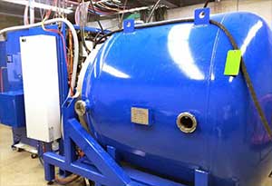
While generally rad-hardened electronics are widely available, electronics specifically qualified for functionality in high neutron radiation environments are very rare, due in part to the limited amount of qualified neutron testing facilities in the world, and in part to the high costs currently associated with neutron testing and evaluation. Phoenix’s engineers would have to conduct their own tests on electronic components in order to clear them for use in their neutron generators, and the very same neutron source housed in their Fitchburg facility, the Phoenix Neutron Imaging Center, made for the perfect proving ground.
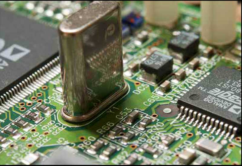
While designing a neutron generator for a client, Phoenix’s engineers calculated that over the course of one year of operation, the electronics would be subjected to a total neutron fluence (neutrons per square centimeter) on the order of 1012 neutrons/cm2. To demonstrate the effects of neutron radiation on typical unshielded electronics, Phoenix’s engineers arranged an experiment to simulate one year of neutron exposure with a commercial off-the-shelf power supply, fitting the operational environment for a system under production for one of Phoenix’s clients. The power supply failed in just twenty minutes under neutron bombardment, corresponding to an effective operational lifetime of under ten days.
The Importance of Neutron Radiation Survivability Testing Capabilities
Accelerated radiation survivability testing of circuits and systems intended for use in high-radiation environments allows engineers to ensure that radiation hardening design practices are working as intended to prolong the operational lifespan of systems and circuits in high-radiation environments. By expanding access to radiation survivability testing capabilities, the immense cost associated with designing and developing sufficiently rad-hardened systems can be lowered. This is vital for bringing down the material and operational costs of critical applications of neutron radiation.
Environments rich in neutron radiation include neutron radiographic and tomographic imaging systems, medical radioisotope production systems, and fusion reactors. In particular, one of the issues currently holding back the development of fusion energy is an extremely limited capacity to simulate the massive amounts of neutron radiation within these environments. Public and private institutions alike working to develop nuclear fusion as a powerful, carbon-neutral source of energy require shielding materials and electronic components capable of withstanding the intense neutron output of a power-generating fusion reactor. Facilities capable of simulating the expected neutron fluence in a fusion reactor are an absolute necessity for designing and developing these materials.
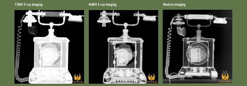
X-rays and neutrons interact with materials differently, creating unique images. This rotary phone is comprised of many dense and light materials. The lower-energy 170 kV X-ray beam could not penetrate the denser materials of the phone. The higher-energy 440 kV X-ray beam could penetrate the denser materials, but was too high-energy to create an image of the lighter materials. The neutron beam could penetrate dense materials but not light materials, creating an image that shows more detail of the phone’s inner workings than either X-ray image could on its own. This is what makes neutron radiography such a powerful complementary tool to X-ray radiography in materials science, materials research. and non-destructive testing applications.